This is an interview published last month in PCB007, where Dan beaulieu interviewed John Johnson
It’s always good to catch up with old friends, especially when you can start working together. I recently spoke with with my friend John Johnson, who has joined American Standard Circuits as the director of business development. At ASC, John will be using the Averatek A-SAP process that he was previously involved with. He shares some of his background and provides insight on the best ways to use this semi-additive PCB fabrication process that opens the capability window for forming trace and space. This process enables ultra-fine lines.
Dan Beaulieu: John good to talk to you again. Congratulations on your new appointment. How did that come about?
John Johnson: Thanks Dan. Over the years I had the chance to get to know Anaya Vardya and Gordhan Patel, and have watched American Standard Circuits grow into the company it is today. In my last position with Averatek I had worked closely on technology integration with ASC’s engineering and operations team. So, when the opportunity arose to join the team at ASC, I didn’t hesitate. I have been impressed with the variety of high tech boards they build and knew that I could add value to their efforts.
Beaulieu: What will you be focusing on at first? Mostly Averatek A-SAP™ process or other technology?
Johnson: My job title is not solely a traditional sales and marketing focus. As I have worked on a variety of challenging technology in my past and with my involvement with Averatek’s A-SAP process, a lot of my focus will be to assist the team in realization of those difficult designs. This will be more time spent with engineering and process development as well as assisting customers with those designs to make them more manufacturable.
Beaulieu: What is your background? Tell us a little about yourself.
Johnson: I have held a lot of roles related to materials and circuit boards manufacturing. I have worked with large companies like GE, Honeywell, Memorex, and Burroughs, and smaller ones where I had ownership, such as a sales rep firm and Electrotek. I have had titles of R&D engineer, quality engineer, senior process engineer, QA manager, sales rep, director of sales, general manager, president, VP of sales, and customer support and now director of business development. From an education standpoint, I have a Bachelor of Science degree in chemistry from Michigan Technological University and a Master of Science degree in organic chemistry from The Ohio State University. Over the years I have added business classes at the University of Wisconsin Eau Claire (which were invaluable, and it amazes me why chemistry curriculum don’t mandate some of these) and countless development seminars in management, quality, sales, and more.
Hard to sum up 44 years in our industry. There have been lots of change and one has to constantly learn new things. That is what I enjoy most about our industry. I have often referred to this as an adrenaline business.
Beaulieu: I know you come fresh from Averatek. What were your duties there?
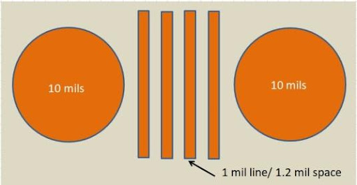
Johnson: My time there was focused on working with existing and prospective licensees on process integration and development using the A-SAP technology and working with the team at Averatek, Santa Clara in process development. This technology is extremely key to our industry, especially in North America where it allows for ultra-fine line production with minimal investment. When I was working with one of the licensees with advanced photolithography, we were able to reproduce half-mil lines and spaces (12.5-micron lines/spaces) with ease.
Beaulieu: I also know that ASC is a licensee to the A-SAP process. I assume you will be doing developing that market as well right?
Johnson: Yes, that is one of the main focus points for me in this role. The sales team at ASC is bringing in a lot of opportunities but as part of Averatek’s support, they also have opportunities coming our way.
Beaulieu: Can you describe that process including its benefits?
Johnson: The A-SAP process is a semi-additive PCB fabrication process that opens the capability window for forming trace and space. This process enables ultra-fine lines; ASC can now offer 25-micron line and space. Beyond this obvious benefit, the process itself, which is now defined by photolithography rather than etching, also has signal integrity benefits even at larger feature sizes.
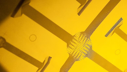
Specific to our medical market, because this process begins building conductors from base dielectric rather than copper, other metals can be used to form the conductive patterns. There is a lot of interest in flexible circuits using gold and platinum as the conductive metal for a more biocompatible solution.
The process in general is very easy to use and a basic installation only needs a series of tanks for the chemistry. The line is scalable for higher volumes and can be set up with an automatic hoist.
Beaulieu: What kind of technologies are best suited for this process?
Johnson: As I noted on an earlier comment, it is not just for fine lines. If a design really needs tight impedance control, the A-SAP process can deliver very tight control to the designed impedance- certainly less than 5% difference provided the dielectric constant and construction is correct. Where signal integrity can be an issue, the trace cross-sectional area can be very close to design and does not vary to the standard processing issues in control of the etched line width. Ninety-nine percent of an A-SAP processed line is plated, and less than 1% is actually etch defined. Build up technologies also work well as generally good adhesion is achieved to the dielectric and these designs are already focused on ultra-fine lines.
The A-SAP process can produce line widths as fine as the photolithography method will allow. The newest imaging equipment will be sub 10 microns. Package substrates already can benefit from the technology.
Beaulieu: How about medical electronics? I saw that it was especially suitable for that area of technology.
Johnson: Medical electronics don’t like to have copper or nickel where the human body can contact them. The Averatek A-SAP process has an adaptation that will allow for using other noble metals which with the body doesn’t have an issue. The Averatek chemistry adheres very well to LCP and adhesive less polyimide films. These items have been used in the body.
More and more we see the integration of medical electronics in the body: neural implants, glucose monitoring, heart monitors and pacemakers. All these can benefit from this technology. ASC is poised to benefit and is adding the medical ISO 13485 approval soon.
Most important, even on the larger medical instrumentation, the ever-shrinking component footprint will drive the need for ultra-fine line capability to build their circuit boards too.
Beaulieu: John, what is your plan for the next three to five years?
Johnson: My plan for is to have a lot of fun with ASC. I have always enjoyed our industry, so having “fun” is easy. ASC has a lot of forward thinking plans and I believe that I can contribute to the team achieving the growth and technology advancement that they desire.
Beaulieu: How do you see the market today?
Johnson: The market for circuit boards today is ever changing. It seems we have finally realized that as a nation it is not too smart to be dependent solely on Asia for all we need in both chips and boards. COVID-19 also has helped with that awareness. All the “saber rattling” that we see in the world today—will all of this end up benefiting our industry? Not if we sit by the sideline and not capitalize on the opportunity the government is affording us.
It is encouraging as well to see the strength in the North American board industry. I believe this will be more than a flash in the pan. We need to invest however, now more than ever. Technology is changing faster than ever. Boards of the future will have ultra-fine lines. BGAs with less than 0.5 mm pitch will guarantee that.
Beaulieu: John, it’s time to wrap up. Any final thoughts?
Johnson: Dan, thanks for taking the time to chat. I think you personally have done a lot to help companies over the years with your columns and trying to provoke thought for the ones who care about this challenging industry. Thanks for all the effort.
Beaulieu: Thank you, John. You’re very kind to say that.